Our paper on hybrid integration of SiV- centres with GaP PhCs has been published in Nanoletters!
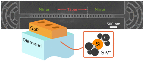
Optically addressable solid-state defects are emerging as some of the most promising qubit platforms for quantum networks. Maximizing photon-defect interaction by nanophotonic cavity coupling is key to network efficiency. We demonstrate fabrication of gallium phosphide 1-D photonic crystal waveguide cavities on a silicon oxide carrier and subsequent integration with implanted silicon-vacancy (SiV) centers in diamond using a stamp-transfer technique. The stamping process avoids diamond etching and allows fine-tuning of the cavities prior to integration. After transfer to diamond, we measure cavity quality factors (Q) of up to 8900 and perform resonant excitation of single SiV centers coupled to these cavities. For a cavity with a Q of 4100, we observe a 3-fold lifetime reduction on-resonance. These results indicate promise for high photon-defect interaction in a platform which avoids fabrication of the quantum defect host crystal.