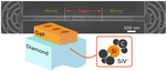
Alexander Abulnaga

Alexander Abulnaga

Doctoral Candidate

Princeton University

Biography

I am a final-year PhD candidate working under the supervision of Nathalie de Leon in the department of Electrical Engineering at Princeton University. My research focuses on the design and fabrication of hybrid III-V on Diamond nanophotonic devices for coupling to neutral silicon vacancy (SiV0) centres. Currently I am investigating the stabilization of bulk implanted SiV0 centres through chemical surface termination, co-doping, and strain engineering. In parallel, I am fabricating 1D GaAs photonic crystal cavities for purcell-enhanced coupling to SiV0, and AlGaAs-on-Diamond ring resonators for frequency conversion of SiV0 emission to the telecom band.

I received my BASc in Electrical Engineering at the University of British Columbia in Vancouver, Canada. My thesis work was performed under the supervision of John Madden and investigated the fabrication of soft-electronics sensors for use in a smart bedsheet. During my undergraduate studies I also worked with Jorge Santiago-Aviles at the University of Pennsylvania through an NSF REU on synthesizing biocompatible piezoelectric nanofibres for use in a novel noninvasive ear surgery procedure.

Interests

  • Nanophotonics
  • Nonlinear Optics
  • Quantum Optics

Education

  • MA in Electrical Engineering, 2020

    Princeton University

  • BASc in Electrical Engineering, 2018

    The University of British Columbia

Recent Posts

A wonderful internship at the AWS Center for Quantum Networking!

This past summer I had the fortune to work at the AWS Center for Quantum Networking as a Quantum Research Intern. At AWS I split my time between device design and spectroscopy of quantum systems.

Our paper on hybrid integration of SiV- centres with GaP PhCs has been published in Nanoletters!

Optically addressable solid-state defects are emerging as some of the most promising qubit platforms for quantum networks. Maximizing photon-defect interaction by nanophotonic cavity coupling is key to network efficiency. We demonstrate fabrication of gallium phosphide 1-D photonic crystal waveguide cavities on a silicon oxide carrier and subsequent integration with implanted silicon-vacancy (SiV) centers in diamond using a stamp-transfer technique.
Our paper on hybrid integration of SiV- centres with GaP PhCs has been published in Nanoletters!

Our paper on hybrid III-V on diamond photonics for quantum nodes has been published in Optics Express!

Integrating atomic quantum memories based on color centers in diamond with on-chip photonic devices would enable entanglement distribution over long distances. However, efforts towards integration have been challenging because color centers can be highly sensitive to their environment, and their properties degrade in nanofabricated structures.
Our paper on hybrid III-V on diamond photonics for quantum nodes has been published in Optics Express!

Recent & Upcoming Talks

Contact